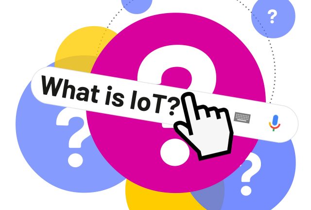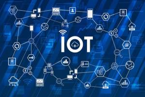
The Internet of Things (IOT) has attracted a large amount of interest from a wide variety of people across the technology food chain. And as so many things in today’s electronics environment, the underlying principles can be attributed to Moore’s Law.
However, says Robert H. Reuss, not in the way so many other advances in electronics are. Rather, than the constant scaling that is the hallmark of Moore’s Law, the growing interest and applications for the Internet of Things might be attributed to what might be called “No Moore”. The excellent review presented by researchers from PARC in “From Printed Transistors to Printed Smart Systems” covers the key issues, challenges and, advances and why their approach might be characterised as No Moore.
Printed transistors and other devices and their interconnections integrated to form systems are an unconventional approach to fabrication of electronics and are not based and driven by Moore’s Law, hence “No Moore”. Rather than making devices smaller, printed electronics was identified and developed as a means to make electronics bigger, initially displays, but then other applications such as photovoltaic panels and area lighting as well, as discussed in the PARC article.
There are several types of printing that have been developed over many years. While the details of the printing process vary, what is important is that materials can be distributed over large areas very rapidly (think newsprint). So, if your goal is large area electronics, printing represents an attractive tool. With the advent of digital printing, the elimination of a physical mask becomes even more attractive. The advantage of the approach is that many different materials can be used as “inks” and can be printed on a wide variety of substrates from glass to plastic to paper. There are many factors to consider with this approach as discussed by Street et al. However, the end result would be lightweight, low cost, bendable, even conformal electronics distributed over large areas if needed.
Unfortunately, while printed electronics is an exciting prospect from a manufacturing perspective, it has significant limitations from an applications perspective. The technology is limited by electrical properties and feature size perspectives and thus is challenged to meet the requirements of many electrical applications beyond displays, PV, and lighting. The factors that must be addressed to achieve adequate electrical functionality are nicely described by PARC. Further, the opportunity for printed electronics is to address applications that don’t demand the high performance that Si provides, but provide functionality that Si-based solutions cannot is highlighted. These applications include wearable electronics (lighter weight, more comfortable, and non-obtrusive), item tags (novel substrates, lightweight, and low cost/disposable), and distributed sensors/actuators (such as EM, pressure, chemical, radiation) that might be integrated into structures for health and safety.
These last set of applications are of course where the connection to IOT arises. If ubiquitous sensors on people, structures, and items are to be interconnected with each other by the internet, then sensors (and their interface electronics) with attributes such as lightweight, low cost/disposable, and novel form factors will be needed. Adequate, but not necessarily, high performance operation would of course be needed and consistent with performance as described in “Smart Systems” paper.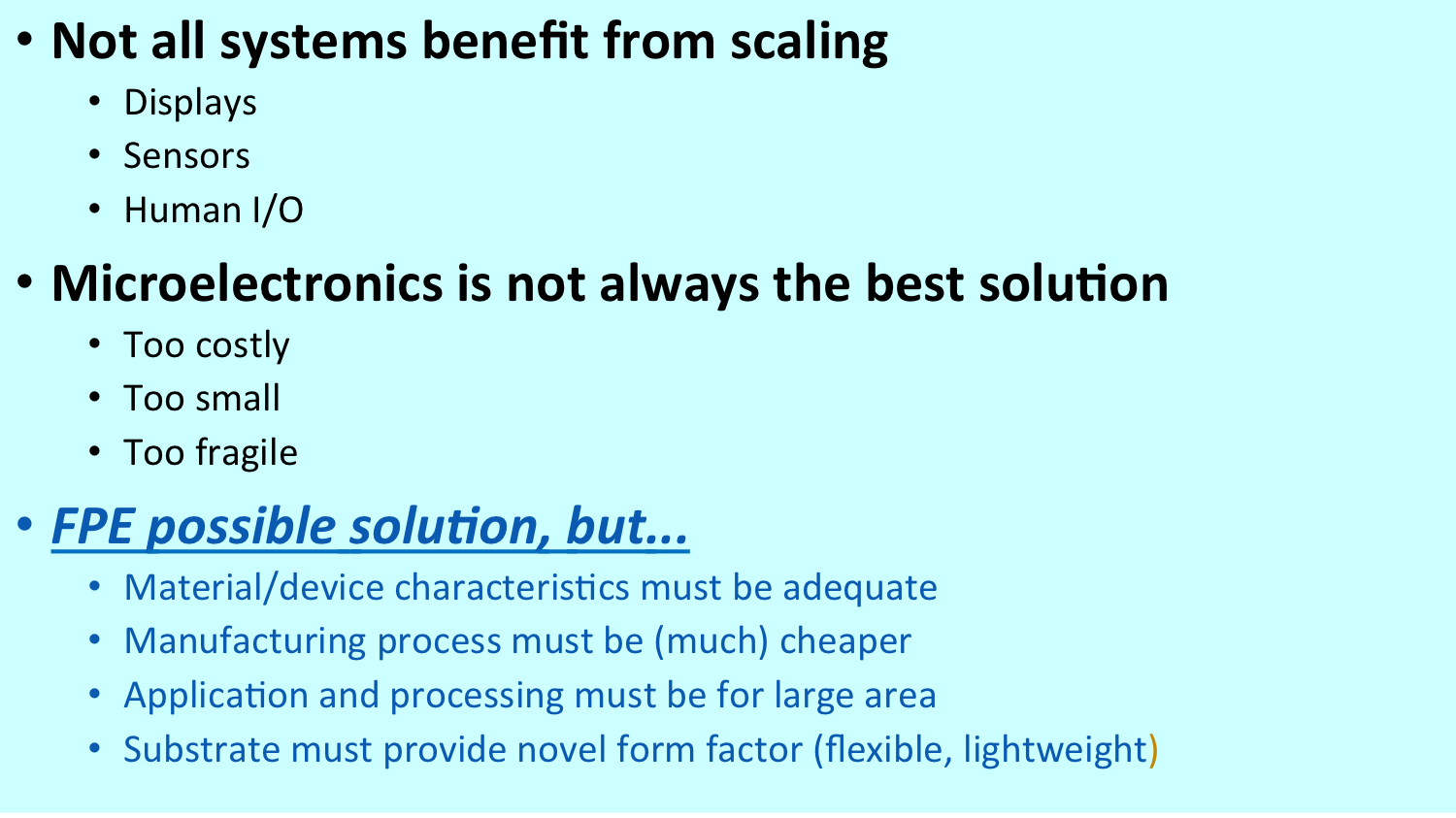
However, what options are available if system performance requirements are more than what printed electronics can provide, yet the attributes of low cost, lightweight, and novel form factors are attractive/required for the application? The Printed Smart System review offers an interesting approach to combining the two in what has been called “More Than Moore”. Si technology has demonstrated an amazing ability to be applied to a wide range of applications, so why not just integrate the two so the sensor is as smart and flexible as the application demands. As always, there are challenges and details to be worked out, some of which are described in the review.
All elements of the electronics community are interested in IOT and closely examining what directions it will take and how they can play. The PARC team has described one possible route to realise some of the critical hardware that will be needed. Their discussion provides valuable insights into solutions that offer flexibility, high volume, and low cost for a wide variety of applications.
The author of this blog is Dr. Robert H. Reuss.
About the author:
Robert H. Reuss received the Ph.D. degree in chemistry from Drexel University, Philadelphia, PA, USA, in 1971. As an Independent Consultant since 2007, he has provide technical evaluation and guidance to government agencies, defense contractors, and commercial suppliers on variety of electronics programs to include flexible electronics, wearable electronics, and photovoltaics. As a DARPA Pro- gram Manager in the Microsystems Technology Office from 2001 to 2006, he was responsible for several research thrusts into fabrication of flexible, large area electronics including high mobility TFTs for digital and RF applications and organic photovoltaics. Prior to joining DARPA, he spent 20 years in various technology and research management positions with Motorola. He has published over 50 papers and has been awarded 13 U.S. patents. His technology interests lie in the area of application of materials and electrochemistry technologies for advanced microelectronic applications and microsystems integration as well as large area electronics.
Comment on this article below or via Twitter: @IoTNow_ OR @jcIoTnow